Famous Kicad Worksheet Layout Editor Ideas. Web new documentation project for kicad. You will see kicad project manager window opened.
Beginner's Guide to KiCad from learn.sparkfun.com
The board will look right but will be centered over the top left corner of. Kicad has a number of user interface behaviors that are common to all the different editor windows. I’d suggest some playing with the worksheet layout editor:
Create And Edit Worksheet Files.
Kicad's schematic editor supports everything from the most basic schematic to a complex hierarchical design with hundreds of sheets. You will see kicad project manager window opened. Click on tools, and then 'run pcbnew', or through a keyboard.
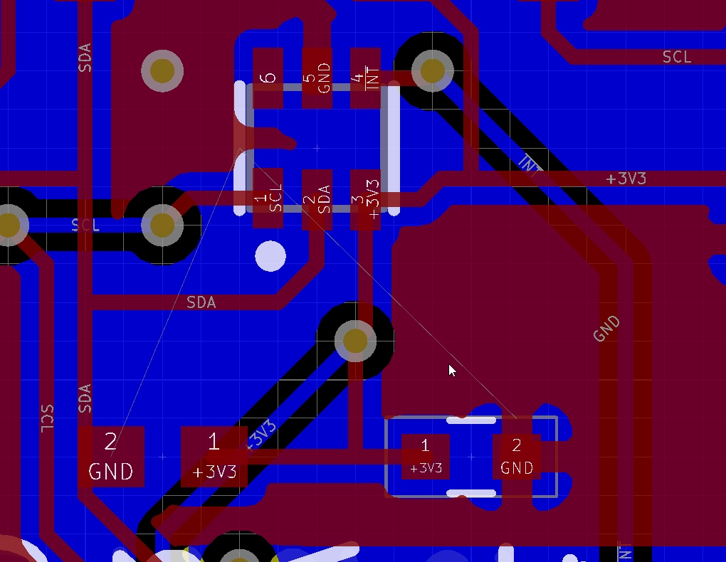
Click On Pcb Layout Editor (Pcbnew) Button.
Web editing a pcb layout. The board will look right but will be centered over the top left corner of. Web kicad copy/pasting and hotkey inconsistencies summary of my post:
In This Editor, You Can Edit The Symbol Fields In Bulk, Instead Of Doing So Individual For Each Symbol In The Symbol’s Properties Window.
Something like this should appear: In there you can change those field names. It facilitates the design and simulation of electronic hardware.
Kicad Has A Number Of User Interface Behaviors That Are Common To All The Different Editor Windows.
Web you can support me on patreon here: Make sure that you have selected the back silkscreen layer (“b.silks”) from the. I thought i would point out the inconsistencies of the ui for.
You Can Also Start Pcbnew Through The Menu.
Web new documentation project for kicad. Work sheet files are used to change the default border and. [eeschema/libraries] after this line, append: